Perovskite solar cells are attracting interest as lower-cost, high-efficiency alternatives to silicon photovoltaics, but defects in their thin films hinder charge transport, waste energy, and reduce device stability.
One approach to mitigate these defects is passivation treatment, in which simple salts or organic molecules are introduced into the perovskite film so that small molecules or ions bind to defect sites and limit their impact on electrical conduction. However, most existing characterization techniques only probe the film surface or provide averaged macroscopic measurements, making it difficult to confirm how well different passivation strategies work inside the film volume.
Researchers at the Ningbo Institute of Materials Technology and Engineering (NIMTE) of the Chinese Academy of Sciences have now developed a three-dimensional electrical imaging method that directly visualizes how defect passivation operates within perovskite layers. The study, published on December 31 in the journal Newton, reports that this method can map charge transport throughout the film and link these microscopic features to solar cell performance.
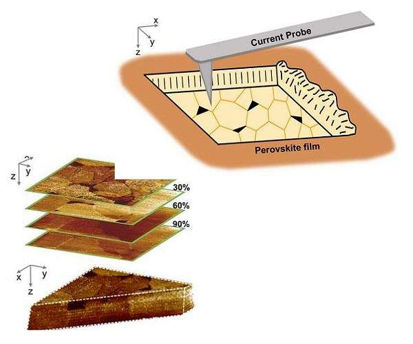
The technique relies on tomographic conductive atomic force microscopy, or TC-AFM, which measures local electrical conductivity while the instrument sequentially removes ultrathin layers from the perovskite film. By stacking the conductivity data acquired at each depth, the team reconstructs a three-dimensional map of current distribution and charge transport pathways with nanoscale spatial resolution.
Using TC-AFM, the researchers compared perovskite films processed with different passivation strategies and directly observed changes in their internal electrical behavior. Films without passivation showed widespread low-conductivity regions that obstruct charge flow, whereas bulk passivation reduced these resistive domains within the film, especially along grain boundaries.
Surface passivation produced a different profile, primarily improving conductivity near the top interface of the film, which is important for integration into complete device architectures. When both bulk and surface passivation were applied together, the films displayed the most uniform and continuous conductive networks, with the remaining low-conductivity zones largely restricted to the surface.
"These microscopic electrical characteristics are closely correlated with the resulting solar cell performance, establishing a direct link between 3D charge transport within the film and overall device efficiency," noted Prof. XIAO Chuanxiao, a corresponding author of the study.
By delivering a direct three-dimensional view of charge-carrier migration in perovskite layers, the new method provides a tool for assessing and refining passivation strategies. The authors report that this approach can guide the rational design of higher-quality perovskite materials and support the development of more efficient and stable perovskite solar cells, as well as other thin-film electronic and optoelectronic devices.
Research Report:Three-dimensional mapping of electrical behavior in perovskite films using tomographic conductive atomic force microscopy