 |
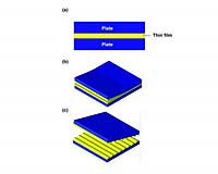
Princeton NJ (SPX) Sep 04, 2007 Creating ultrasmall grooves on microchips -- a key part of many modern technologies -- is about to become as easy as making a sandwich, using a new process invented by Princeton engineers. The simple, low-cost technique results in the self-formation of periodic lines, or gratings, separated by as few as 60 nanometers -- less than one ten-thousandth of a millimeter -- on microchips. Features of this size have many uses in optical, biological and electronic devices, including the alignment of liquid crystals in displays. The researchers will publish their findings Sept. 2 in the online version of Nature Nanotechnology. "It's like magic," said electrical engineer Stephen Chou, the Joseph C. Elgin Professor of Engineering. "This is a fundamentally different way of making nanopatterns." The process, called fracture-induced structuring, is as easy as one-two-three. First, a thin polymer film is painted onto a rigid plate, such as a silicon wafer. Then, a second plate is placed on top, creating a polymer sandwich that is heated to ensure adhesion. Finally, the two plates are pried apart. As the film fractures, it automatically breaks into two complementary sets of nanoscale gratings, one on each plate. The distance between the lines, called the period, is four times the film thickness. The ease of creating these lines is in marked contrast to traditional fabrication methods, which typically use a beam of electrons, ions, or a mechanical tip to "draw" the lines into a surface. These methods are serial processes which are extremely slow and therefore only suitable for areas one square millimeter or smaller. Other techniques suitable for larger areas have difficulties achieving small grating periods or producing a high yield, or they require complex and expensive processes. Fracture-induced structuring is not only simple and fast, but it enables patterning over a much larger area. The researchers have already demonstrated the ability of the technique to create gratings over several square centimeters, and the patterning of much large areas should be possible with further optimization of the technique. "It's remarkable - and counterintuitive - that fracturing creates these regular patterns," said chemical engineering professor and dean of Princeton's graduate school William Russel. Russel and his graduate student Leonard Pease III teamed with Chou and his graduate students Paru Deshpande and Ying Wang to develop the technique. A patent application has been filed on the process, which the researchers say is economically feasible for large-scale use in industry. The gratings generated by the fracturing process also could be used in conjunction with existing patterning methods. For example, the nanoimprinting method invented by Chou in the 1990s can use the gratings generated by fracture-induced structuring to create a mold that enables mass duplication of patterns with high precision at low cost. As with many scientific discoveries, the fracture-induced structuring process was happened upon accidentally. Graduate students in the Chou and Russel groups were trying to use instabilities in various molten polymers (in essence, melted plastic) to create patterns when they discovered instead that fracturing a solid polymer film can generate the gratings automatically. The team seized upon this finding and established the optimal conditions for grating formation. Next, the group plans to explore the fundamental science behind the process and investigate the interplays of various forces at such a small scale, according to Chou. "And, we want to push the limit and see how small we can go," he said. Related Links Princeton University, Engineering School Computer Chip Architecture, Technology and Manufacture Nano Technology News From SpaceMart.com
 Washington DC (SPX) Aug 22, 2007
In the Sept. 3 issue of Optical Society of America's Optics Express, published online today, researchers announce that they have built the world's first "mode-locked silicon evanescent laser." Mode-locked evanescent lasers can deliver stable short pulses of laser light that are useful for many optical applications, including high-speed data transmission, multiple wavelength generation, remote sensing (LIDAR) and highly accurate optical clocks. |
|
| The content herein, unless otherwise known to be public domain, are Copyright Space.TV Corporation. AFP and UPI Wire Stories are copyright Agence France-Presse and United Press International. ESA Portal Reports are copyright European Space Agency. All NASA sourced material is public domain. Additional copyrights may apply in whole or part to other bona fide parties. Advertising does not imply endorsement, agreement or approval of any opinions, statements or information provided by Space.TV Corp on any Web page published or hosted by Space.TV Corp. Privacy Statement |