| . |  |
. |
|
|
. |
by Staff Writers Hoboken NJ (SPX) Sep 08, 2011
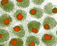
In the quest to exploit unique properties at the nanoscale, scientists at Stevens Institute of Technology have developed a novel technique for creating uniform arrays of metallic nanostructures. A team of faculty and students in the Department of Physics and Engineering Physics, led by Dr. Stefan Strauf, appropriated methods from holographic lithography to demonstrate a new approach for scaling up the fabrication of plasmonic nanogap arrays while simultaneously reducing costs and infrastructure. A paper on the technique recently appeared in Nano Letters 11, 2715 (2011). "Prof. Strauf is doing research at the forefront of physics," says Dr. Rainer Martini, Department Director for Physics and Engineering Physics. "His lab is producing research breakthroughs with impact well beyond his own field as well as providing excellent learning and publishing opportunities for graduate and undergraduate students." Plasmonic nanogap arrays are essentially uniformly placed metallic nanostructures which feature a tiny air gap between neighbors. By creating strongly confined electrical fields under optical illumination, these tiny air gaps allow scientists to use the arrays in a variety of applications, particularly in the miniaturization of photonic circuits and ultrasensitive sensing. Such sensors could be used to detect the presence of specific proteins or chemicals down to the level of single molecules, or employed in high-resolution microscopy. Nanophotonic circuits, able to transmit huge amounts of information, are considered crucial to bring about the exaflop processing era and a new generation in computing power. Established fabrication techniques for nanogap arrays have focused on serial methods, which are time-consuming, have a low throughput, and are consequently expensive. Holographic lithography (HL), an optical approach that takes advantage of interference patterns of laser beams to create periodic patterns, had been previously demonstrated to create sub wavelength features. Dr. Strauf's team advanced the HL methodology by using four-beam interference and the concept of a compound lattice to create tunable twin motive shapes into a polymer template, resulting in metallic air gaps down to 7 nm, seventy times smaller than the wavelengths of the blue laser light utilized to write the features. The Stevens scientists extended the utility of HL to create gaps with results comparable to laborious serial fabrication techniques such as electron beam lithography or focused ion beam milling. Besides being a simpler and more cost-effective production method, their technique does not require a clean room and currently achieves 90% uniformity in the array pattern. Therefore, these innovations provide the foundation for making high-quality, large-scale arrays at a greater speed and lower cost than previously realizable. "This research project provided me with an opportunity to become an expert with the HL technique," says Xi Zhang, the first author of the Nano Letters article and a PhD candidate. Xi and her fellow students are now measuring the surface enhanced Raman scattering (SERS) effects that result from these arrays and continue to improve the uniformity of the arrays during fabrication. "We just got some excellent results from first SERS experiment, and certainly there are more papers to follow up," she says.
Dr. Strauf is Director of the NanoPhotonics Laboratory (NPL) at Stevens, where he oversees cutting-edge research in the fields of solid-state nanophotonics and nanoelectronics. Research at the lab includes the development of fabrication methods for nanoscale materials and quantum device applications.
Recent NPL projects have resulted in papers published on quantum dots and graphene. The lab has received project funding from the Air Force Office of Scientific Research and two National Science Foundation instrumentation grants. Dr. Strauf is also the recipient of the prestigious NSF CAREER Award. Related Links Physics and Engineering at Stevens Institute of Technology Nano Technology News From SpaceMart.com Computer Chip Architecture, Technology and Manufacture
|
. |
|
| The content herein, unless otherwise known to be public domain, are Copyright 1995-2011 - Space Media Network. AFP and UPI Wire Stories are copyright Agence France-Presse and United Press International. ESA Portal Reports are copyright European Space Agency. All NASA sourced material is public domain. Additional copyrights may apply in whole or part to other bona fide parties. Advertising does not imply endorsement,agreement or approval of any opinions, statements or information provided by Space Media Network on any Web page published or hosted by Space Media Network. Privacy Statement |

 del.icio.us
 Digg
Digg Reddit
 Google